Newcomers’ Tutorial
Note
This guide assumes that the reader has some basic knowledge of Digital Design, ASIC, the JSON format and RTL.
Designing an ASIC is a complex and fascinating process that entails various steps, from idea to the fabrication data. This process is filled with engineering challenges that require expertise and attention to detail. The entire process requires significant expertise and experience in chip design and can take several months to complete. The ASIC design flow is crucial to ensure successful ASIC design. It is based on a comprehensive understanding of ASIC specifications, requirements, low-power design, and performance. Engineers can streamline the process and meet crucial time-to-market goals by following a proven ASIC design flow. Each stage of the ASIC design cycle is supported by powerful EDA (Electronic Design Automation) tools that facilitate the implementation of the design. The following are examples of steps needed to realize an ASIC.
Design Entry: The design is described is described using a hardware description language such as Verilog. For digital design, modeling is typically done at the register transfer level,
Functional Verification: A combination of HDL simulation and formal verification to ensure that the design behaves as expected against the requirements. It is essential to perform functional verification on both the input RTL and the gate-level netlist for the circuit.
Synthesis: In this step, the HDL description is converted into a circuit of the logic cells called the Netlist.
Layout/Physical Synthesis: Also called Physical Implementation. In this step, the logic circuit is converted into a layout of the photo masks used for fabrication. This complex step involves several sub-steps typically automated using its flow. These steps include Floorplanning, Placement, Clock-tree synthesis and Routing. Because Placement and Routing are the most time-consuming operations, sometimes we refer to this step as “Placement and Routing”, or PnR.
Signoff: The final stage in the rigorous journey of an ASIC’s design; it ensures your creation functions flawlessly, operates efficiently, and ultimately delivers on its promise before sending your chip blueprint off to be etched in silicon.
Do note that these are only the broad strokes — there are many other steps that are quite important when making a chip — scan chain insertion, pattern generation, one or more ECOs, et cetera.

Fig. 2 ASIC Flow
What is LibreLane?
LibreLane is a powerful and versatile infrastructure library that enables the
construction of digital ASIC physical implementation flows based on open-source
and commercial EDA tools. It includes a reference flow (Classic) that is
constructed entirely using open-source EDA tools — abstracting their behavior
and allowing the user to configure them using a single file (See Figure 1).
LibreLane also supports extending or modifying flows using Python scripts and
utilities. Here are some of the key benefits of using LibreLane:
Flexibility and extensibility: LibreLane is designed to be flexible and extensible, allowing designers to customize flows to meet their specific needs. This can be done by writing Python scripts and utilities, or by modifying the existing configuration file.
Open source: LibreLane is an open-source project, which means that it is freely available to use and modify. This makes it a good choice for designers who are looking for a cost-effective and transparent solution.
Community support: LibreLane capitalizes on both it and its predecessor’s (OpenLane’s) existing community of users and contributors. This means that there is a wealth of resources available to help designers get started and troubleshoot any problems they encounter.
Installation
Follow the instructions in Nix-based Installation to install Nix and set up the binary cache.
Open a terminal and clone LibreLane as follows:
$ git clone https://github.com/librelane/librelane/ ~/librelane
Invoke
nix-shell, which will make all the packages bundled with LibreLane available to your shell.$ nix-shell ~/librelane/shell.nix
Some packages will be downloaded (about 3GiB) and afterwards, the terminal prompt should change to:
[nix-shell:~/librelane]$Important
From now on; all commands assume that you are inside the
nix-shell.Run the smoke test to ensure everything is fine. As part of the test, the open-source sky130 process design kit.
[nix-shell:~/librelane]$ librelane --log-level ERROR --condensed --show-progress-bar --smoke-test
That’s it. Everything is ready. Now, let’s try LibreLane.
Running the default flow
PM32 example
We are going to use a simple design: a 32-bit parallel multiplier which performs a simple multiplication between MP and MC and outputs the product on a bus P. MP32 uses a serial-by-parallel multiplier, a serializer, a deserializer, and a control unit. The block diagram of the PM32 is shown in the next figure.
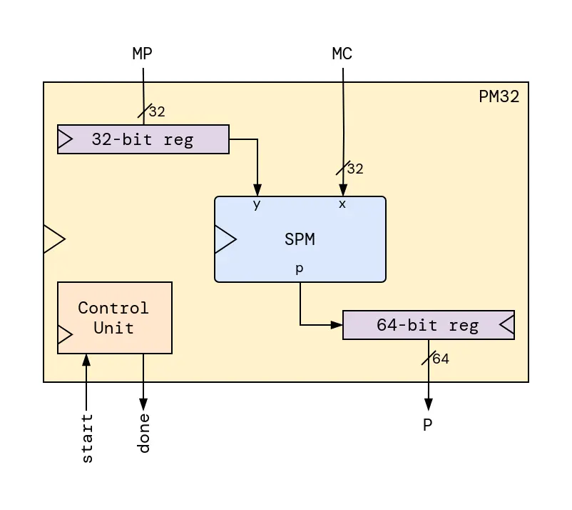
Fig. 3 PM32 (32-bit parallel multiplier)
The serial-by-parallel signed 32-bit multiplier SPM block inside the PM32
performs a simple shift-add algorithm, where the parallel input x is
multiplied by each bit of the serial input y as it is shifted in. The product
is generated and serially output on the wire p. Check
this paper for more information
about the SPM.
RTL
The source RTL of the design will consist of 2 files, which are spm.v
and pm32.v.
pm32.v
// A signed 32x32 Multiplier utilizing SPM
//
// Copyright 2016, mshalan@aucegypt.edu

`timescale		    1ns/1ps
`default_nettype    none

module pm32 (
    input wire          clk,
    input wire          rst,
    input wire          start,
    input wire  [31:0]  mc,
    input wire  [31:0]  mp,
    output reg  [63:0]  p,
    output wire         done
);
    wire        pw;
    reg [31:0]  Y;
    reg [7:0]   cnt, ncnt;
    reg [1:0]   state, nstate;

    localparam  IDLE=0, RUNNING=1, DONE=2;

    always @(posedge clk or posedge rst)
        if(rst)
            state  <= IDLE;
        else
            state <= nstate;

    always @*
        case(state)
            IDLE    :   if(start) nstate = RUNNING; else nstate = IDLE;
            RUNNING :   if(cnt == 64) nstate = DONE; else nstate = RUNNING;
            DONE    :   if(start) nstate = RUNNING; else nstate = DONE;
            default :   nstate = IDLE;
        endcase

    always @(posedge clk)
        cnt <= ncnt;

    always @*
        case(state)
            IDLE    :   ncnt = 0;
            RUNNING :   ncnt = cnt + 1;
            DONE    :   ncnt = 0;
            default :   ncnt = 0;
        endcase

    always @(posedge clk or posedge rst)
        if(rst)
            Y <= 32'b0;
        else if((start == 1'b1))
            Y <= mp;
        else if(state==RUNNING)
            Y <= (Y >> 1);

    always @(posedge clk or posedge rst)
        if(rst)
            p <= 64'b0;
        else if(start)
            p <= 64'b0;
        else if(state==RUNNING)
            p <= {pw, p[63:1]};

    wire y = (state==RUNNING) ? Y[0] : 1'b0;

    spm #(.SIZE(32)) spm32(
        .clk(clk),
        .rst(rst),
        .x(mc),
        .y(y),
        .p(pw)
    );

    assign done = (state == DONE);

endmodule
spm.v
/*
    A Serial-Parallel Multiplier (SPM)
    Modeled after the design outlined by ATML for their
    AT6000 FPGA in application notes DOC0716 and DOC0529:
        - https://ww1.microchip.com/downloads/en/AppNotes/DOC0529.PDF
        - https://ww1.microchip.com/downloads/en/AppNotes/DOC0716.PDF

    Implemented by mshalan@aucegypt.edu, 2016
*/

`timescale		    1ns/1ps
`default_nettype    none

module spm #(parameter SIZE = 32)(
    input wire              clk,
    input wire              rst,
    input wire              y,
    input wire [SIZE-1:0]   x,
    output wire             p
);
    wire [SIZE-1:1]     pp;
    wire [SIZE-1:0]     xy;

    genvar i;

    CSADD csa0 (.clk(clk), .rst(rst), .x(x[0]&y), .y(pp[1]), .sum(p));

    generate
        for(i=1; i<SIZE-1; i=i+1) begin
            CSADD csa (.clk(clk), .rst(rst), .x(x[i]&y), .y(pp[i+1]), .sum(pp[i]));
        end
    endgenerate

    TCMP tcmp (.clk(clk), .rst(rst), .a(x[SIZE-1]&y), .s(pp[SIZE-1]));

endmodule


// Carry Save Adder
module CSADD(
    input wire  clk,
    input wire  rst,
    input wire  x,
    input wire  y,
    output reg  sum
);

    reg sc;

    // Half Adders logic
    wire hsum1, hco1;
    assign hsum1 = y ^ sc;
    assign hco1 = y & sc;

    wire hsum2, hco2;
    assign hsum2 = x ^ hsum1;
    assign hco2 = x & hsum1;

    always @(posedge clk or posedge rst) begin
        if (rst) begin
            sum <= 1'b0;
            sc <= 1'b0;
        end
        else begin
            sum <= hsum2;
            sc <= hco1 ^ hco2;
        end
    end
endmodule

// 2's Complement
module TCMP (
    input wire  clk,
    input wire  rst,
    input wire  a,
    output reg  s
);

    reg z;

    always @(posedge clk or posedge rst) begin
        if (rst) begin
            s <= 1'b0;
            z <= 1'b0;
        end
        else begin
            z <= a | z;
            s <= a ^ z;
        end
    end

endmodule
Configuration
Designs in LibreLane have configuration files. A configuration file contains
values set by the user for various librelane.config.Variable(s). With
them, you control the flows. This is the configuration file for the
pm32 design:
config.json
{
  "DESIGN_NAME": "pm32",
  "VERILOG_FILES": ["dir::pm32.v", "dir::spm.v"],
  "CLOCK_PERIOD": 25,
  "CLOCK_PORT": "clk"
}
In general, for any design, at a minimum you need to specify the following variables:
See also
Check out the Classic flow’s documentation for information about all available variables.
Running the flow
Create a directory to add our source files to:
[nix-shell:~/librelane]$ mkdir -p ~/my_designs/pm32
Create the file
~/my_designs/pm32/config.jsonand add configuration content to it.Create the files
~/my_designs/pm32/pm32.v,~/my_designs/pm32/spm.v, and add RTL content to them.Run the following command:
[nix-shell:~/librelane]$ librelane ~/my_designs/pm32/config.json
Tip
Double-checking: are you inside a nix-shell? Your terminal prompt
should look like this:
[nix-shell:~/librelane]$
If not, enter the following command in your terminal:
$ nix-shell ~/librelane/shell.nix
Checking the results
Viewing the Layout
To open the final GDSII layout run this command:
[nix-shell:~/librelane]$ librelane --last-run --flow openinklayout ~/my_designs/pm32/config.json
This opens KLayout and you should be able to see the following:
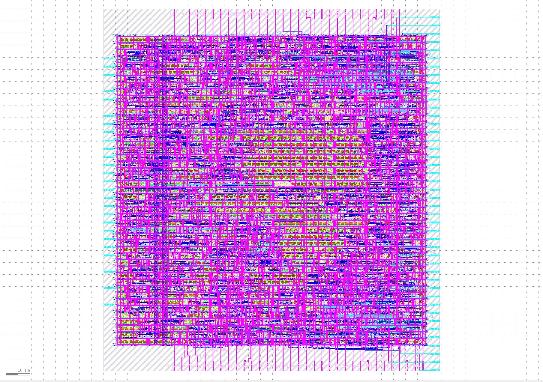
Fig. 4 Final layout of pm32
If you wish to view the layout in the OpenROAD GUI, try this command instead:
[nix-shell:~/librelane]$ librelane --last-run --flow openinopenroad ~/my_designs/pm32/config.json
Run directory
You’ll find that a run directory (named something like
runs/RUN_2023-12-27_16-59-15) was created when you ran LibreLane.
By default, LibreLane runs a Flow composed of a
sequence of Step(s). Each step has its
separate directory within the run directory.
For example, the OpenROAD.TapEndCapInsertion Step creates the following
directory 18-openroad-tapendcapinsertion.
A step directory has log files, report files, metrics and output artifacts created by the step.
For example, these are the contents of 18-openroad-tapendcapinsertion:
18-openroad-tapendcapinsertion/
├── COMMANDS
├── config.json
├── _env.tcl
├── openroad-tapendcapinsertion.log
├── openroad-tapendcapinsertion.process_stats.json
├── or_metrics_out.json
├── pm32.def
├── pm32.nl.v
├── pm32.odb
├── pm32.pnl.v
├── pm32.sdc
├── runtime.txt
├── state_in.json
└── state_out.json
Here is a small description of each of those files:
Directory of contents
COMMANDS: any commands run by the stepconfig.json: a configuration file with all variables accessible by this Step*.log: log files of subprocesses run by the step*.process_stats.json: statistics about total elapsed time and resource consumption of subprocessesstate_in.json: contains a dictionary of design layout formats (such as DEF files) and design metrics available as inputs to a stepstate_out.json: contains the valuestate_out.jsonafter updates by the step- e.g. if a step generates a new DEF file, it would be updated instate_out.json.pm32.nl.v: A Verilog gate-level netlist generated by the step without power connectionspm32.pnl.v: A Verilog gate-level netlist generated by the step with power connectionspm32.odb: The current state of the layout saved in the OpenROAD database formatpm32.def: The current state of the layout saved in the DEF formatpm32.sdc: Current constraints on the design saved in the SDC format.
Tip
Using state_out.json, you can view the layout at intermediate steps as well!
[nix-shell:~/librelane]$ librelane --last-run --flow openinklayout ~/my_designs/pm32/config.json --with-initial-state ~/my_designs/pm32/runs/RUN_2023-12-27_16-59-15/18-openroad-tapendcapinsertion/state_out.json"
The run directory is composed of many of these step directories:
RUN_2023-12-27_16-59-15
├── 01-verilator-lint
├── 02-checker-linttimingconstructs
├── 03-checker-linterrors
├── 04-checker-lintwarnings
├── 05-yosys-jsonheader
├── 06-yosys-synthesis
├── 07-checker-yosysunmappedcells
├── 08-checker-yosyssynthchecks
├── 09-checker-netlistassignstatements
├── 10-openroad-checksdcfiles
├── 11-openroad-checkmacroinstances
├── 12-openroad-staprepnr
├── 13-openroad-floorplan
├── 14-odb-checkmacroantennaproperties
├── 15-odb-setpowerconnections
⋮
├── final/
├── tmp
├── error.log
├── info.log
├── resolved.json
└── warning.log
Final Results
Inside the run directory, you may have noticed there is another, non-specific
step folder named final.
final contains several directories that contain all the different layout
views produced by the flow. It looks like this:
final
├── def/
├── gds/
├── json_h/
├── klayout_gds/
├── lef/
├── lib/
├── mag/
├── mag_gds/
├── nl/
├── odb/
├── pnl/
├── sdc/
├── sdf/
├── spef/
├── spice/
├── vh/
├── metrics.csv
└── metrics.json
Moreover, it contains metrics.csv and metric.json which represent the final
metrics in JSON and CSV formats.
Signoff Steps
An ASIC design’s signoff is the last phase of its implementation. It involves physical and timing verifications before committing to the silicon manufacturing process, which is commonly known as “design tape-out”.
LibreLane runs a couple of Step(s) for the final signoff.
DRC
DRC stands for Design Rule Checking which checks, against rules set by
chip foundries, that the layout has to satisfy in order to be manufacturable,
such as checking for minimum allowed spacing between two met1 shapes.
LibreLane runs two DRC steps using Magic and KLayout: Magic.DRC and
KLayout.DRC. Both tools have blind spots that are covered by the other tools.
Both the layout and what is known as a PDK’s DRC deck are processed by the tools running DRC, as shown in the diagram below:
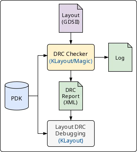
Fig. 5 DRC (Design Rule Checking) Flow
If DRC violations are found; LibreLane will generate an error reporting the total count of violations found by each Step.
To view DRC errors graphically, you may open the layout as follows:
[nix-shell:~/librelane]$ librelane --last-run --flow openinklayout ~/my_designs/pm32/config.json
Then in the menu bar select Tools ► Marker Browser. A new window should open.
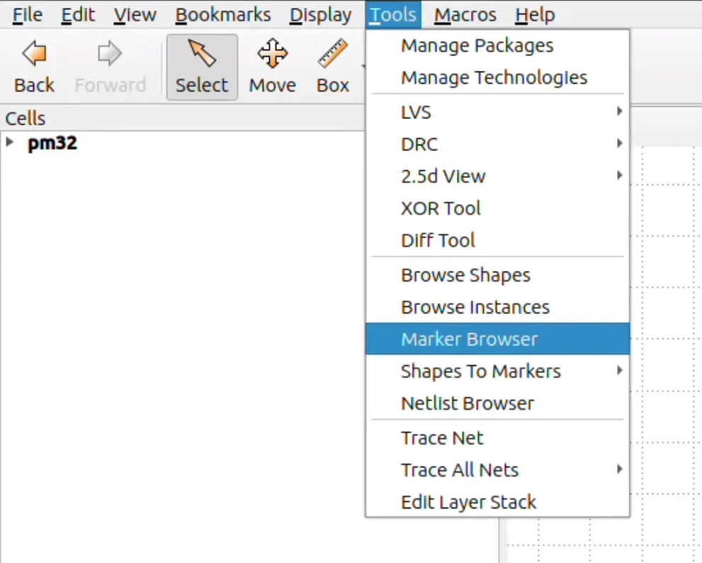
Fig. 6 Tools ► Marker Browser
Click File ► Open and then select the DRC report file, of which you’ll find two:
One under 52-magic-drc/reports/drc.klayout.xml and the other under
63-klayout-drc/report/drc.klayout.xml.
Tip
The initial number in 63-klayout-drc (63) may vary according to the
flow’s configuration.
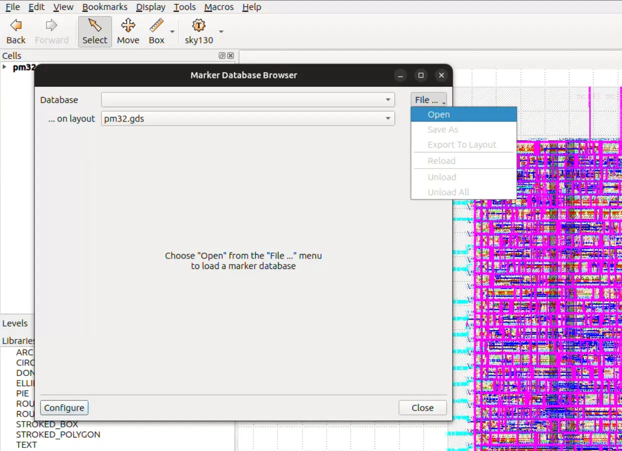
Fig. 7 Opening DRC xml file
LVS
LVS stands for Layout Versus Schematic. It compares the layout GDSII or DEF/LEF, with the schematic which is usually in Verilog, ensuring that connectivity in both views matches. Sometimes, user configuration or even the tools have errors and such a check is important to catch them.
Common LVS errors include but are not limited to:
Shorts: Two or more wires that should not be connected have been and must be separated. The most problematic is power and ground shorts.
Opens: Wires or components that should be connected are left dangling or only partially connected. These must be connected properly.
Missing Components: An expected component has been left out of the layout.
Netgen.LVS is the Step run for LVS using a tool called Netgen. First,
the layout is converted to SPICE netlist. Next, the layout and the
schematic are inputted to Netgen, as shown in the diagram below:
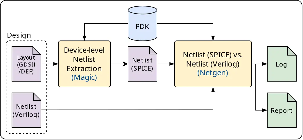
Fig. 8 LVS (Layout-versus-Schematic) Flow
Netgen will generate multiple files that can be browsed in case of LVS errors.
As with all Step(s), these will be inside the Step’s directory.
You would want to look at netgen-lvs.log which has a summary of the results of
LVS. Ideally, you would find the following at the end of this log file:
Final result:
Circuits match uniquely.
In case of errors, there is also lvs.netgen.rpt which is more detailed. Inside it,
you will find tables comparing nodes between the layout and the schematic. On
the left is the layout (GDS) and the schematic (Verilog) is on the other side.
Here is a sample of these tables:
Subcircuit summary:
Circuit 1: pm32                             |Circuit 2: pm32
-------------------------------------------|-------------------------------------------
sky130_fd_sc_hd__tapvpwrvgnd_1 (102->1)    |sky130_fd_sc_hd__tapvpwrvgnd_1 (102->1)
sky130_fd_sc_hd__decap_3 (144->1)          |sky130_fd_sc_hd__decap_3 (144->1)
sky130_fd_sc_hd__inv_2 (64)                |sky130_fd_sc_hd__inv_2 (64)
sky130_fd_sc_hd__nand2_1 (31)              |sky130_fd_sc_hd__nand2_1 (31)
sky130_fd_sc_hd__dfrtp_1 (64)              |sky130_fd_sc_hd__dfrtp_1 (64)
sky130_ef_sc_hd__decap_12 (132->1)         |sky130_ef_sc_hd__decap_12 (132->1)
STA
STA stands for Static Timing Analysis. The STA tool identifies the design timing paths and then calculates the data’s earliest and latest actual and required arrival times at every timing path endpoint. If the data arrives after (in case of setup checking) or before (hold checking) it is required, then we have a timing violation (negative slack). STA makes sure that a circuit will correctly perform its function (but tells nothing about the correctness of that function.)
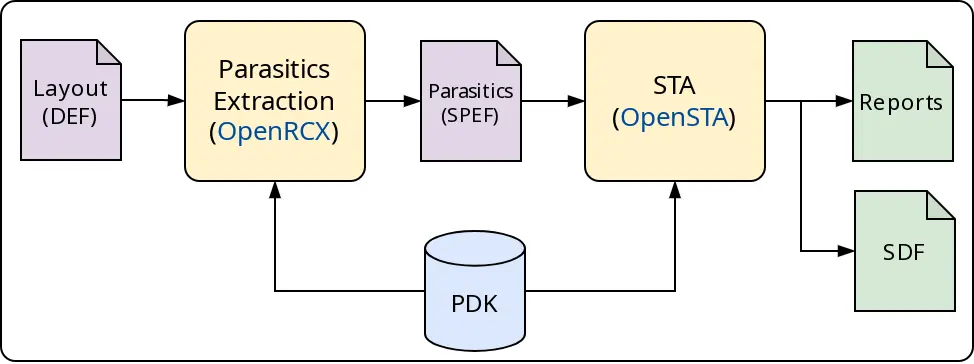
Fig. 9 STA (Static Timing Analysis) Flow
The default flow runs a step called OpenROAD.STAPostPNR for STA
signoff.
Note
During the Classic flow the step OpenROAD.STAMidPNR is ran
multiple times.
The results are not as accurate as OpenROAD.STAPostPNR since the design
is not fully implemented yet. However, they provide a better sense of the impact
multiple stages of the flow (such as optimizations steps) on STA results for the
design.
Inside the Step directory, there is a file called summary.rpt which summarizes
important metrics for each IPVT timing corner:
┏━━━━━━━━━━━━━━━━━━┳━━━━━━━━━━━━━━━━━━┳━━━━━━━━━━━━━━━━━━┳━━━━━━━━━━┳━━━━━━━━━━━━━━━━━┳━━━━━━━━━━━━━━━━━━━━━┳━━━━━━━━━━━━━━━━━━━┳━━━━━━━━━━━━━━━━━━┳━━━━━━━━━━━┳━━━━━━━━━━━━━━━━━━┳━━━━━━━━━━━━━━━━━━━━━┳━━━━━━━━━━━━━━━━━━━━┳━━━━━━━━━━━━━━━━━━━━━┓
┃ Corner/Group     ┃ Hold Worst Slack ┃ Reg to Reg Paths ┃ Hold TNS ┃ Hold Violations ┃ of which Reg to Reg ┃ Setup Worst Slack ┃ Reg to Reg Paths ┃ Setup TNS ┃ Setup Violations ┃ of which Reg to Reg ┃ Max Cap Violations ┃ Max Slew Violations ┃
┡━━━━━━━━━━━━━━━━━━╇━━━━━━━━━━━━━━━━━━╇━━━━━━━━━━━━━━━━━━╇━━━━━━━━━━╇━━━━━━━━━━━━━━━━━╇━━━━━━━━━━━━━━━━━━━━━╇━━━━━━━━━━━━━━━━━━━╇━━━━━━━━━━━━━━━━━━╇━━━━━━━━━━━╇━━━━━━━━━━━━━━━━━━╇━━━━━━━━━━━━━━━━━━━━━╇━━━━━━━━━━━━━━━━━━━━╇━━━━━━━━━━━━━━━━━━━━━┩
│ Overall          │ 0.1097           │ 0.1097           │ 0.0000   │ 0               │ 0                   │ 16.2115           │ 21.3285          │ 0.0000    │ 0                │ 0                   │ 0                  │ 0                   │
│ nom_tt_025C_1v80 │ 0.3314           │ 0.3314           │ 0.0000   │ 0               │ 0                   │ 17.9815           │ 23.0789          │ 0.0000    │ 0                │ 0                   │ 0                  │ 0                   │
│ nom_ss_100C_1v60 │ 0.9203           │ 0.9203           │ 0.0000   │ 0               │ 0                   │ 16.2759           │ 21.3412          │ 0.0000    │ 0                │ 0                   │ 0                  │ 0                   │
│ nom_ff_n40C_1v95 │ 0.1125           │ 0.1125           │ 0.0000   │ 0               │ 0                   │ 18.5942           │ 23.6426          │ 0.0000    │ 0                │ 0                   │ 0                  │ 0                   │
│ min_tt_025C_1v80 │ 0.3275           │ 0.3275           │ 0.0000   │ 0               │ 0                   │ 18.0196           │ 23.0863          │ 0.0000    │ 0                │ 0                   │ 0                  │ 0                   │
│ min_ss_100C_1v60 │ 0.9154           │ 0.9154           │ 0.0000   │ 0               │ 0                   │ 16.3522           │ 21.3516          │ 0.0000    │ 0                │ 0                   │ 0                  │ 0                   │
│ min_ff_n40C_1v95 │ 0.1097           │ 0.1097           │ 0.0000   │ 0               │ 0                   │ 18.6191           │ 23.6477          │ 0.0000    │ 0                │ 0                   │ 0                  │ 0                   │
│ max_tt_025C_1v80 │ 0.3356           │ 0.3356           │ 0.0000   │ 0               │ 0                   │ 17.9481           │ 23.0714          │ 0.0000    │ 0                │ 0                   │ 0                  │ 0                   │
│ max_ss_100C_1v60 │ 0.9274           │ 0.9274           │ 0.0000   │ 0               │ 0                   │ 16.2115           │ 21.3285          │ 0.0000    │ 0                │ 0                   │ 0                  │ 0                   │
│ max_ff_n40C_1v95 │ 0.1153           │ 0.1153           │ 0.0000   │ 0               │ 0                   │ 18.5732           │ 23.6374          │ 0.0000    │ 0                │ 0                   │ 0                  │ 0                   │
└──────────────────┴──────────────────┴──────────────────┴──────────┴─────────────────┴─────────────────────┴───────────────────┴──────────────────┴───────────┴──────────────────┴─────────────────────┴────────────────────┴─────────────────────┘
More about IPVT corners
IPVT corners stands for Interconnect, Process, Voltage, and Temperature corners. Interconnect corners take into account variations in interconnect width, thickness, and height, as well as the dielectric properties of the materials surrounding them. Interconnect variations affect the signal delay, power dissipation, and cross-talks. PVT corners represent the extreme conditions of manufacturing process variations, operating voltage fluctuations, and temperature ranges an IC might experience. These corners are used to simulate the worst-case scenarios to ensure that the IC functions correctly under all possible conditions. For instance, a slow process corner combined with low voltage, high temperature, and maximum interconnect delay could represent a worst-case scenario for timing, leading to slower transistor speeds hence more likely to have setup violations. On the other hand, a fast process corner combined with high voltage, low temperature, and min interconnects could represent the fastest scenario for timing, which is more likely to have hold violations. If we go back to the STA summary table, the worst setup slack is in the max_ss_100C_1v60 which has the maximum interconnect delay, slow device process, high temperature (100 Celsius), and low voltage (1.60V). Alternatively, the worst hold slack is in the min_ff_n40C_1v95 which has the minimum interconnect delay, fast device process, low temperature (negative 40 Celsius), and high voltage (1.95V).
There is also a directory per corner inside the Step directory which contains
all the log files and reports generated for each IPVT corner.
54-openroad-stapostpnr/
└── nom_tt_025C_1v80/
    ├── checks.rpt
    ├── filter_unannotated.log
    ├── filter_unannotated.process_stats.json
    ├── filter_unannotated_metrics.json
    ├── max.rpt
    ├── min.rpt
    ├── power.rpt
    ├── skew.max.rpt
    ├── skew.min.rpt
    ├── pm32__nom_tt_025C_1v80.lib
    ├── pm32__nom_tt_025C_1v80.sdf
    ├── sta.log
    ├── sta.process_stats.json
    ├── tns.max.rpt
    ├── tns.min.rpt
    ├── violator_list.rpt
    ├── wns.max.rpt
    ├── wns.min.rpt
    ├── ws.max.rpt
    └── ws.min.rpt
Here is a small description of each file:
sta.log: Full log file generated by STA which is divided into the following report filesmin.rpt: Constrained paths for hold checks.max.rpt: Constrained paths for setup checks.skew.min.rpt: Maximum clock skew for hold checks.skew.max.rpt: Maximum clock skew for setup checks.tns.min.rpt: Total negative hold slack.tns.max.rpt: Total negative setup slack.wns.min.rpt: Worst negative hold slack.wns.max.rpt: Worst negative setup slack.ws.min.rpt: Worst hold slack.ws.max.rpt: Worst setup slack.violator_list.rptSetup and hold violator endpoints.checks.rpt: It contains a summary of the following checks:Max capacitance violations
Max slew violations
Max fanout violations
Unconstrained paths
Unannotated and partially annotated nets
Checks the SDC for combinational loops, register/latch with multiple clocks or no clocks, ports missing input delay, and generated clocks
Worst setup or hold violating path
See also
Check out our STA and timing closure guide for a deeper dive into what you can do to achieve timing closure when violations actually occur.
Antenna Check
Long metal wire segments that are connected to a transistor gate may damage the transistor’s thin gate oxide during the fabrication process due to its collection of charges from the processing environment. This is called the antenna effect (Also, called Plasma Induced Gate Oxide Damage). Chip foundries normally supply antenna rules, which are rules that must be obeyed to avoid this problem. The rules limit the ratio of collection area and drainage (thin oxide) area. Antenna effect can be avoided by instructing the router to use short wire segments and to create bridges to disconnect long from transistor gates during fabrication. This approach is not used by LibreLane as OpenROAD routers don’t support this methodology. Instead, LibreLane uses another approach that involves the insertion of an antenna diode (provided as a standard cell) next to the cell input pin that suffers from the antenna effect. Antenna diode cell has a reversed biased diode which can drain out the charge without affecting the transistor circuitry.
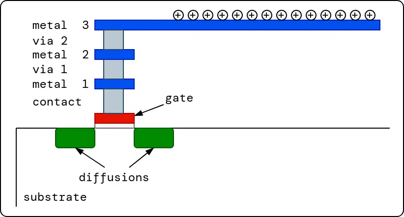
Fig. 10 Antenna effect
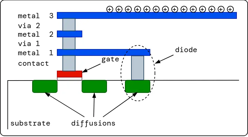
Fig. 11 Antenna diode insertion
The default flow runs a step called OpenROAD.CheckAntennas to check for
antenna rules violations.
Note
The checker runs thrice during the flow:
Once immediately after global routing
Once as part of the
OpenROAD.RepairAntennascomposite stepDuring signoff
First two are ran to see the impact of antenna repair step.
Inside the step directory of OpenROAD.CheckAntennas, there is a reports
directory that contains two files; the full antenna check report from
OpenROAD and a summary table of antenna violations:
┏━━━━━━━━━━━━━━━━━━┳━━━━━━━━━━┳━━━━━━━━━┳━━━━━━━━┳━━━━━━━━━━━━━┳━━━━━━━┓
┃ Partial/Required ┃ Required ┃ Partial ┃ Net    ┃ Pin         ┃ Layer ┃
┡━━━━━━━━━━━━━━━━━━╇━━━━━━━━━━╇━━━━━━━━━╇━━━━━━━━╇━━━━━━━━━━━━━╇━━━━━━━┩
│ 1.43             │ 400.00   │ 573.48  │ net162 │ output162/A │ met3  │
│ 1.28             │ 400.00   │ 513.90  │ net56  │ _1758_/A1   │ met3  │
└──────────────────┴──────────┴─────────┴────────┴─────────────┴───────┘
Adding custom pin placement configuration
As seen in the previous layout, the pins of the pm32 macro are placed
randomly. If this macro will be integrated into a larger macro or chip, the pin
placement should be according to the top-level connectivity. For example, if the
clock pin will be derived from a clocking macro that will be placed on the east
side of this macro, then the clock pin in the pm32 should be placed on the
east side. In order to change pin placement, we can add a pin placement
configuration file to our flow as follows:
Create the file
~/my_designs/pm32/pin_order.cfgConfigure the pin placement as follows.
pin_order.cfg
#E
clk
rst
start
done

#S
mc.*
mp.*

#N
p.*
Tip
See the document /reference/pin_placement_cfg.md for more information about configuring pin placements.
Add
"IO_PIN_ORDER_CFG": "dir::pin_order.cfg"to the config.json so the new config file will be like this
config.json
{
  "DESIGN_NAME": "pm32",
  "VERILOG_FILES": ["dir::pm32.v", "dir::spm.v"],
  "CLOCK_PERIOD": 25,
  "CLOCK_PORT": "clk",
  "IO_PIN_ORDER_CFG": "dir::pin_order.cfg"
}
Run the flow again using the following command:
[nix-shell:~/librelane]$ librelane ~/my_designs/pm32/config.json
Check the final layout again using this command:
[nix-shell:~/librelane]$ librelane --last-run --flow openinklayout ~/my_designs/pm32/config.json
Since the configuration file pin_order.cfg has #E then clk, rst,
start, then done, we will find those 4 pins on the east side of the macro.
Similarly, we will find mc and mp buses on the south and p on the north of
the macro.
Fig. 12 Custom IO placed layout